
We all know that in the modern electronics manufacturing field, HDI technology has become a key factor in driving electronic products towards miniaturization and higher performance. The core of HDI technology lies in its unique stack-up design, which not only greatly enhances the space utilization of the circuit board but also significantly strengthens electrical performance and signal integrity.
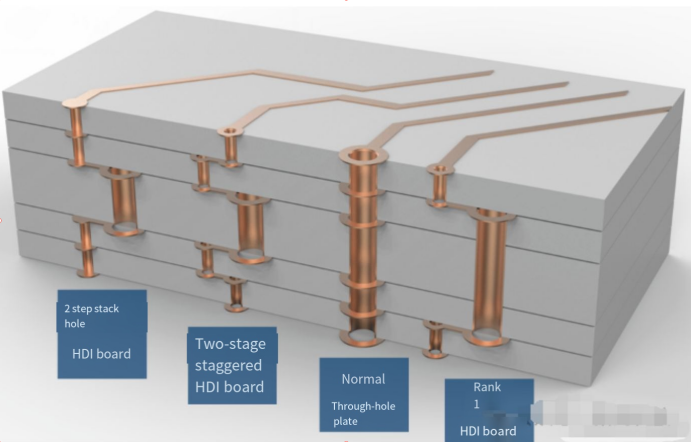
The stack-up design of HDI allows multiple circuit layers to be connected through precisely controlled blind and buried vias, the diameters of which are much smaller than the through-holes of traditional PCBs. This fine connection method not only reduces the volume of the circuit board but also increases the wiring density, allowing more electronic components to be integrated into a limited space.
In addition, the stack-up design of HDI also optimizes the signal transmission path. Since the signal transmission distance is shorter and unnecessary bends and corners are avoided, signal delay and loss are effectively controlled. This is crucial for high-speed electronic devices, as they need to process large amounts of data quickly and accurately.
In the manufacturing process, the stack-up design of HDI also brings many challenges. To achieve high-precision blind and buried via processing and interlayer alignment, manufacturers must adopt advanced laser drilling technology and precise etching equipment. At the same time, to ensure the reliability and stability of the circuit board, it is also necessary to conduct strict testing and verification of materials and processes.
So, what are the HDI stack-up designs? In the next article, we will introduce them in detail.


