
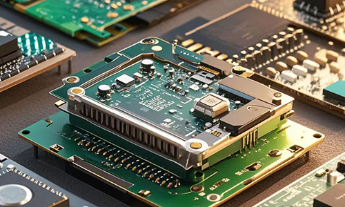
6-layer HDI Communication PCB board is a printed circuit board designed for high-end electronic devices such as smartphones or other cell phones.
Technical Parameters
| Number of layers | 6 | Line width/line spacing | 0.06/0.063mm |
| Product structure | 1+4+1 | Minimum laser drilling aperture | 0.1mm |
| Board thickness | 0.8±0.8mm | Surface treatment | immersion nickel gold |
| Material | EM-285 | / | / |
| WHY US |
||||
 |
 |
 |
||
| Fast Delivery | High Quality | Diversified Customization | ||
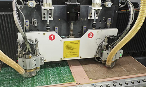
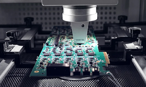
| Factory | ||||
 |
 |
 |
||
| Photoengraving Workshop | Drilling Machine | Electroplating Production Line | ||
| More Information | ||
| Strategic Partners | Application | Certificate |
FAQ
1.Q: What is your minimum order quantity?
A: One piece is enough to place an order.
2.Q: When can I get a quotation after I provide Gerber, product process requirements?
A: Our sales staff will give you a quotation within 1 hour.
3.Q: Why do signals sometimes become incomplete in devices equipped with communication PCB?
A: As design complexity increases, 5G devices may utilize HDI communication PCBs with finer traces and higher-density interconnections. When transmitting high-speed signals, these finer traces may lead to incomplete signals. If such issues occur, please contact our staff to make adjustments for your product.
4.Q: Can your company produce Controlled Depth PCB?
A: We can control the design of drilled holes according to the customer's drawing size requirements to ensure compliance with the customer's drawing requirements.
 10-Layer High-Frequency & High-Speed Communication PCB
 6-layer 5G Communication System AC PCB
 12-layer Second-Generation Communication Receiver System Dedicated AC PCB
 14-layer Communication Receiving AC PCB
 4-Layer PCB for Small Optical Communication Instruments
 2-Layer Communication 5G Antenna PCB


