
6-Layer keyboard communication PCB is a core component designed for wireless gaming keyboards, aiming to provide efficient, stable wireless connection and excellent user experience.
Technical Specifications
| Number of layers | 6 | Ink color | green oil with white characters |
| Material | FR-4 S1141 | Minimum line width/line spacing | 0.1mm/0.1mm |
| Thickness | 3.0mm | Features | controlled depth sinking 2.0MM |
| Copper thickness | 1oz inner layer, 1oz outer layer | Surface treatment | immersion gold |
| WHY US |
||||
 |
 |
 |
||
| Fast Delivery | High Quality | Diversified Customization | ||
| Factory | ||||
 |
 |
 |
||
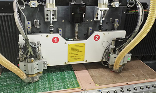
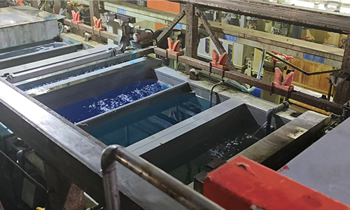
| Photoengraving Workshop | Drilling Machine | Electroplating Production Line | ||
| More Information | ||
| Strategic Partners | Application | Certificate |
FQA
1.Q: How many employees do you have in your factory?
A: More than 500.
2.Q: Are the materials you use environmentally friendly?
A: The materials we use are in accordance with ROHS standard and IPC-4101 standard.
3.Q: What problems can be caused by inaccurate PCB design in mobile phones?
A: If the circuit design lacks a rational layout, it may lead to signal interference and unstable transmission, thereby affecting the performance of the entire phone. Therefore, we need to fully consider the position of each component and the rationality of the wiring during the PCB design phase.
4.Q: Can a lack of strict control during the production process lead to many problems?
A: In the production process, issues such as uneven plating thickness and inaccurate milling can negatively impact the performance of PCB. Therefore, strict control of the production process is key to ensuring quality.
 10-Layer High-Frequency & High-Speed Communication PCB
 6-layer 5G Communication System AC PCB
 12-layer Second-Generation Communication Receiver System Dedicated AC PCB
 14-layer Communication Receiving AC PCB
 4-Layer PCB for Small Optical Communication Instruments
 2-Layer Communication 5G Antenna PCB


