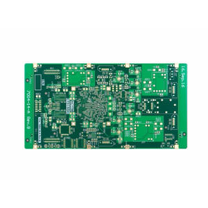
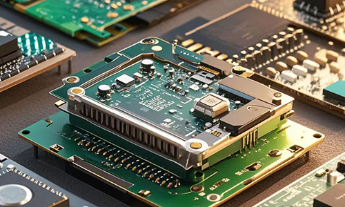
14-layer High-Level PCB is a high-performance PCB designed for complicated and precise medical equipment.
Technical Parameters
| Number of layers | 14L | Minimum aperture | 0.25mm |
| Board thickness | 2.0mm | Minimum line width/line spacing | 0.1mm/0.1mm |
| Material | FR-4 SY1000-2 | Inner copper thickness | 18μm |
| Ink color | green oil with white characters | Outer copper thickness | 35μm |
| Surface treatment | ENIG | Minimum distance from hole to line | 0.2mm |
| WHY US |
||||
 |
 |
 |
||
| Fast Delivery | High Quality | Diversified Customization | ||
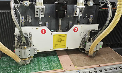
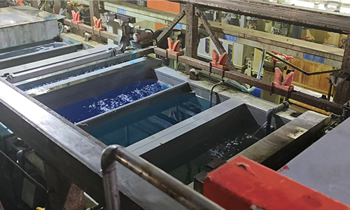
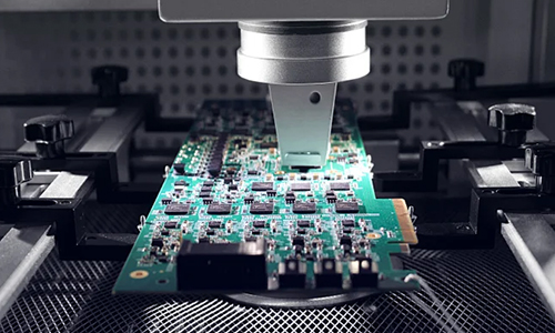
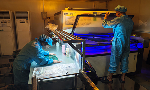
| Factory | ||||
 |
 |
 |
||
| Photoengraving Workshop | Drilling Machine | Electroplating Production Line | ||
| More Information | ||
| Strategic Partners | Application | Certificate |
FAQ
1.Q: Are the materials you use environmentally friendly?
A: The materials we use are in accordance with ROHS standard and IPC-4101 standard.
2.Q: How far is your factory from the nearest airport?
A: About 30 kilometers.
3.Q: Does the chemically plated palladium layer of nickel-palladium-gold PCB completely dissolve in the soldering process?
A: Yes, the chemically plated palladium layer completely dissolves in the solder during the soldering process.
4.Q: Can you do nickel-palladium gold processing?
A: Yes, we can.