
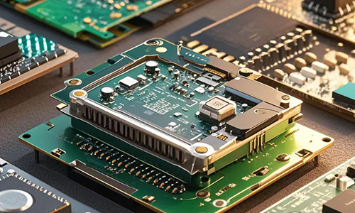
This basic testing PCB is designed for test some small electronic components, it is very widely used in electronic area.
Technical Specifications
| Base material | FR4 | Board material | / |
| Copper foil thickness | 1OZ (outer layer) | Copper thickness | / |
| Number of layers | 2 | Minimum line width and line spacing | 0.05/0.05mm |
| Board thickness | 3.0mm | Minimum aperture | 0.05 |
| Surface treatment | lead-free tin spraying | Process points | / |
| WHY US |
||||
 |
 |
 |
||
| Fast Delivery | High Quality | Diversified Customization | ||
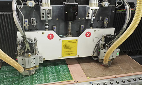
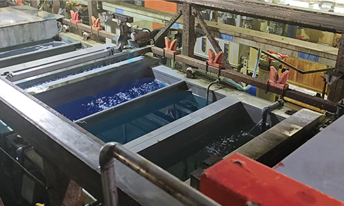
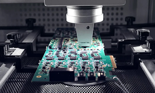
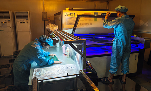
| Factory | ||||
 |
 |
 |
||
| Photoengraving Workshop | Drilling Machine | Electroplating Production Line | ||
| More Information | ||
| Strategic Partners | Application | Certificate |
FAQ
1.Q: Do you have an office address that could be visited?
A: Our office address is Tianyue Building, Bao 'an District, Shenzhen.
2.Q: Will you attend the exhibition to show your products?
A: We are planning on it.
3.Q: How to solve the thermal management issue in electronic PCB?
A: Prevent overheating by reasonable layout and thermal conductive materials.
4.Q: Can you do nickel-palladium gold processing?
A: Yes, we can.


